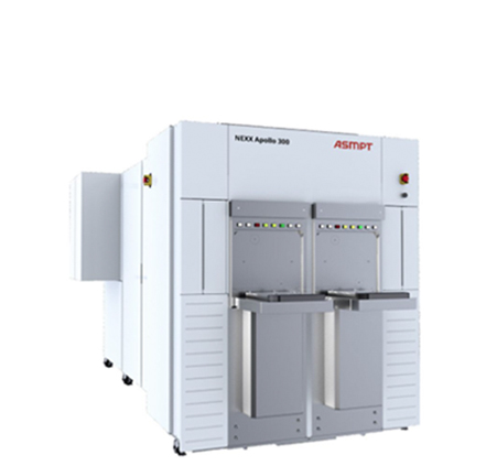
Apollo 300
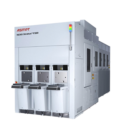
StratusTM P300
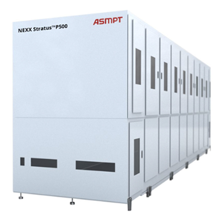
StratusTM P500
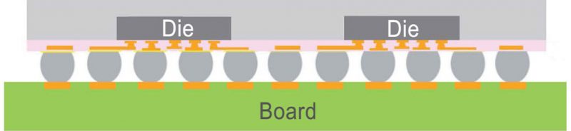
The Fan Out process generally represents the redistribution of the interconnects located inside and outside of the die envelope. The term fan out often includes a variety of assembly methods: embedded wafer level package (WLP), embedded wafer level ball grid array (eWLB), wafer level system in package (WLSiP). The Fan Out process can also embed chip capacitors and inductors and has also been contemplated for 3D die stacking.
The Fan Out technology is often a process of reconstituting a new wafer or panel on all KGD (known good die). KGD are accurately placed and temporarily held on to an interposer with double sided sticky tape or an adhesive. Then, EMC (Embedded Mold Compound) is applied to create a new wafer or panel. Once the new wafer or panel is created then the front-end lithography steppers apply the RDL (Redistribution Layer) connecting and relocating the interconnections. The RDL process demands that increasingly thin PVD seeds be sputtered and finer RDLs be plated with micron accuracy and tight uniformity over the entire wafer or panel substrate. One of the major challenges is finding sputtering and plating machines that can deliver thin, uniform seeds and fine line RDL plating below 10 um L/S uniformly across a variety of large areas.
 Source: Collection of Advanced Packaging reports Yole Développement, 2018 www.i-micronews.com
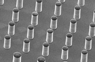
Cu Pillar
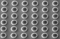
Bumps
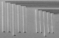
RDL
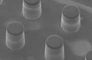
Macro Cu Pillar
Product Offering
ASMPT NEXX offering sputtering and plating wafer and panel level solution for the Fan Out processes. NEXX offers features and options to support both current processes and variations which evolve as the interconnection market matures. NEXX serves the high volume manufacturing portion of the Fan Out market.
Wafer Sputtering – Apollo 300

Apollo Under Bump Metallization (UBM) is an in-line physical vapor deposition system for customers who manufacture multiple advanced packaging features, such as a range of copper redistribution layers (RDL), the Apollo UBM produces both thick and thin films in the most compact footprint on the market.
Benefits
- High throughput sputtering solution for thick and thin films
- Stress management to reduce wafer and die warpage
- Handles multiple wafer sizes
- Safer handling of an array of wafer types
- Up to 5 different metals
- Degas
- DC Pulsed Sputtering
- Backside Gas (BSG)
- Reactive Sputtering
- RF Bias
- ICP and CCP etch Electrostatic chucks
- Bridge tool capability
- Fully configurable
- Processes 300 and 200 mm wafers

For customers who manufacture multiple advanced packaging features including the standard copper pillar interconnects and microbumps. The P300’s high speed wafer handling system delivers the flexibility and extendibility to produce both large and small features.
- Highest productivity plating tool on the market
- Process RDLs, Copper Pillars and TSVs in one tool
- Handles multiple wafer sizes
- Safer handling of an array of wafer types
- Shields make faster plating possible while maintaining good within wafer uniformity
Features
-
- Up to 6 different chemistries
- Various reservoir sizes for high or low volume plating Chemistry stabilizing cell technology (SnAg and Ni)
- ShearPlate Technology
- Up to 30 wafer processing
- Bridge tool capability
- Fully configurable
- Processes 300 and 200 mm wafers
Related products: S300, S200
Panel Plating – StratusTM P500

The StratusTM P500 has been proven to deliver wafer scale plating precision on panels up to 510 x 515 mm at the leading panel makers. This panel scale plating tool is a semiconductor industry game changer because it brings higher quality, wafer level chemistries to glass and epoxy panel substrates.
Benefits
- Highest technology panel plating tool on the market delivering <10 um RDL L/S and an array of advanced packaging features
- Safer handling of thin, bowed and warped panels
- Shields make faster plating possible while maintaining good within panel uniformity
Features
- Up to 5 different chemistries
- Various reservoir sizes for high or low volume plating Membrane cell technology
- ShearPlate Technology
- Segmented anodes
- Single or Dual sided plating
- Bridge tool capability
- Fully configurable
- Processes 510 x 515 mm panels