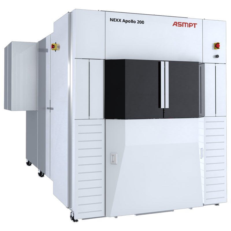
Wafer Sputtering – Apollo 200
PVD 100-200 mm Wafer Processing
Applications
- Configurable for up to 5 metals
- SiC / Power Devices
- UBM/RDL
- RF Filters
- EMI
Features
- Multiple wafer size capability
- Size Change
- Degas/anneal
- ICP/CCP Etch (Optimal Reactive Plasma Treatment)
Substrates
- 100, 150, and 200 mm wafers
- Fragile & thin wafer processing
- Silicon, EMC, Glass, LiNbO3/LiTaO3, GaAs, Bonded
Other Products