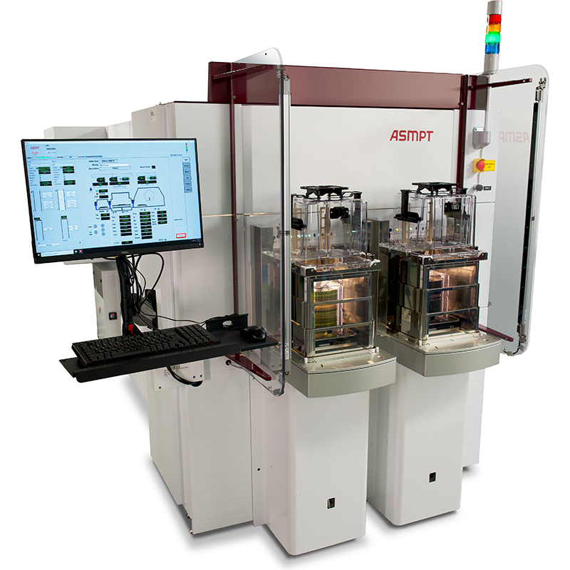
Wafer Sputtering – Apollo 300
PVD 200-300 mm Wafer Processing
Applications
- Configurable for up to 5 metals
- UBM/RDL
- Fan Out
- RF Filters
- Power Devices
Features
- True Bridge tool capability: Size Change
- Degas/Anneal
- ICP/CCP Etch
Substrates
- 200 and 300 mm wafers
- Warped and heavy wafer processing
- Silicon, EMC, RCP, Glass, Bonded
Other Products